0. Basic Knowledge
What is the SMT Process?
SMT (Surface Mount Technology) refers to a series of manufacturing processes performed on the PCB (Printed Circuit Board). It is the most popular technology in the electronics assembly industry.
Surface Mount Technology (SMT) involves mounting surface-mounted components (SMC/SMD) without leads or with short leads onto the surface of PCBs or other substrates. The components are soldered using reflow soldering or wave soldering techniques.
Virtually all electronic products are created by assembling capacitors, resistors, and other electronic components on a PCB according to a designed circuit. Therefore, various types of electronic products require different SMT process flows during manufacturing.
1. Pre-Production Preparation
- A completed PCB sample must be available.
- All components for assembly should be prepared (include extra parts for loss—expect approx. 0.3% loss rate).
- The BOM (Bill of Materials) must be accurate and clearly labeled to prevent procurement mistakes.
- Allocate sufficient processing time. (Typically, one production batch takes around one week.)
- The PCB design origin should not be arbitrarily modified post-panelization; otherwise, the stencil alignment may fail.
2. Factory Safety Measures
- SMT production lines must be protected against electrostatic discharge (ESD).
- Follow ESD protection standards strictly within the SMT workshop.
- Establish a robust anti-static system in the SMT factory.
3. Equipment Introduction
- QFP, BGA Packages, and IC Chips are typically placed using SMT machines.
- DIP (Dual Inline Package) components must be soldered manually.
4. SMT Core Process
1. Solder Paste Printing
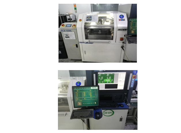
- Solder paste must be stored in a freezer and thawed for 12–24 hours before use.
- Stencil size should be 550–650 mm; too small and the printer may not work.
- SPI (Solder Paste Inspection) is used to detect short circuits, insufficient paste, misalignment, thickness, volume, and area issues.
- Each PCB must pass self-inspection. Printing defects such as excess, insufficient, or offset solder paste are unacceptable.
- Clean the stencil promptly, replenish solder paste as needed, and ensure smooth rolling on the stencil.
Main Equipment:
- Automatic Solder Paste Printer
- 3D Solder Paste Inspection (SPI) Machine
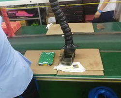
2. Component Placement
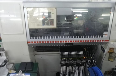
- Placement order: from smaller/lower profile components to larger/higher ones.
- Smaller components occupy one pick-up position, while larger ones may take 2–3 positions, affecting production efficiency.
- Placement programs are compiled and materials are organized into a report (component model, specs, location) to create a reference sample.
Main Equipment:
- Multi-Function Pick and Place Machine
3. Reflow Soldering
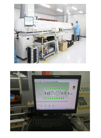
- Reflow ovens typically have 10 temperature zones, high-end models may have 12.
- Zones include: preheat, soak, reflow, and cooling. More zones mean better thermal control.
- Oven temperature is slightly lower than the set value.
- PCB max width: 450 mm
- Check component temperature ratings and notify the factory if special requirements exist.
Main Equipment:
- Reflow Oven (with computer-controlled temperature interface)
4. AOI (Automated Optical Inspection)
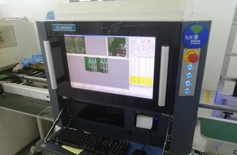
AOI automatically inspects soldered PCBs for defects such as:
- Wrong component
- Missing component
- Polarity reversed
- Extra component
- Misaligned component
- Soldering defects: too much/little solder, cold solder joints, solder balls
- Bent leads, tombstoning, foreign objects
Main Equipment:
- Automated Optical Inspection (AOI) System
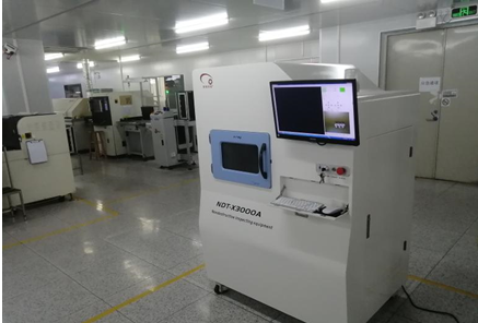
5. X-Ray Inspection
X-ray machines work like projection microscopes using X-rays to image internal structures.
Used for:
- BGA, QFN, LED, semiconductors
- Internal structure analysis (e.g., inaccessible pads)
- Detects differences in material density and atomic number
Main Equipment:
- X-Ray Inspection Machine
6. Final Inspection
- Perform basic visual checks.
- For functional testing, customers must provide test files and specifications.
7. Auxiliary Tools
7.1 Fixture Tools
Used for boards with both THT and SMT parts, preventing component loss during reflow. Critical areas are cut out or exposed as needed.
7.2 PCB Vacuum Cleaner
Used to remove debris from the PCB surface.
7.3 Burn-in Test Rack
Simulates high-temperature environments for aging tests on high-performance electronics (e.g., computers, automotive electronics).
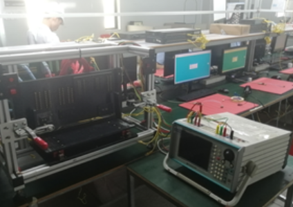
7.4 Test Platform
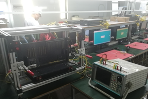
Used for product functional testing.
7.5 Custom Test Fixtures
Designed by the customer based on their schematic to facilitate PCB testing.
7.6 Functional Board Testing
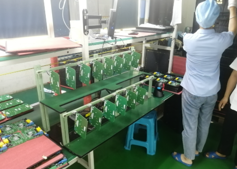
Verify the functionality of the assembled boards.
7.7 Firmware Programming
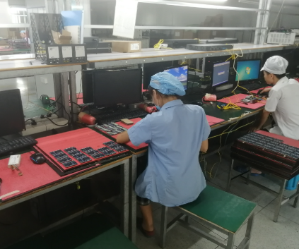
Used to program and verify firmware or software on the assembled boards.
8. Additional Information
Advantages of SMT Assembly:
| Feature | Benefit |
|---|---|
| High Assembly Density | Smaller, lighter electronic products |
| Compact Components | SMDs are about 1/10 the size and weight of traditional through-hole parts |
| Size & Weight Reduction | Up to 40–60% smaller, 60–80% lighter |
| High Reliability | Stronger vibration resistance, lower defect rate |
| Excellent Electrical Performance | Better high-frequency performance, less EMI/RFI |
| High Automation Potential | Improved productivity, lower labor costs |
| Cost Efficiency | Saves up to 30–50% in overall cost |
| Resource Saving | Reduced material, energy, and equipment usage |