BUYSMT – Your Global SMT Equipment & Parts Supplier
What is SMT (Surface Mount Technology)?
Surface Mount Technology (SMT) is the most popular and widely used electronic assembly technique in the electronics manufacturing industry. Also known as Surface Mount Assembly (SMA), SMT involves mounting pinless or short-lead Surface Mount Components (SMCs or SMDs) onto the surface of Printed Circuit Boards (PCBs) or other substrates. The assembly is done through soldering processes such as reflow soldering or wave soldering.
For professional SMT machines and parts, visit BUYSMT SMT Equipment.
What Are the Basic Elements of the SMT Process?
The core SMT manufacturing process includes:
- Solder Paste Printing (Screen Printing)
- Dispensing (Glue Application)
- Pick-and-Place Mounting
- Reflow Soldering
- Cleaning
- Solder Paste Inspection (SPI)
- Quality Inspection
- Rework
1. Solder Paste Printing (Screen Printing)
Applies solder paste or adhesive to PCB pads via a stencil. This step prepares the PCB for component mounting. The key equipment is the screen printer, located at the start of the SMT line.
2. Dispensing
Applies glue or adhesive at specific PCB locations to secure components during assembly. The dispensing machine is placed either before pick-and-place or after inspection stations.
3. Pick-and-Place Mounting
Accurately mounts Surface Mount Components onto the PCB pads. The pick-and-place machine follows solder paste printing on the SMT line.
4. Reflow Soldering
Melts the solder paste to firmly attach components to the PCB. The reflow oven is located downstream of the pick-and-place machine.
5. Cleaning
Removes harmful solder residues like flux from the PCB surface to ensure product safety. Cleaning equipment can be in-line or offline.
6. Solder Paste Inspection (SPI)
Detects defects in solder paste printing such as volume, area, height, misalignment, missing paste, and damage.
7. Quality Inspection
Includes various inspection methods to ensure solder joint and assembly quality:
- Visual magnifiers and microscopes
- In-Circuit Test (ICT)
- Flying Probe Test
- Automated Optical Inspection (AOI)
- X-Ray Inspection Systems
- Functional Testing Equipment
Inspection stations can be placed at suitable points along the SMT line.
8. Rework
Repairs defective PCBs detected during inspection. Equipment includes soldering irons and rework stations, positioned anywhere along the production line.
For detailed SMT equipment, visit BUYSMT SMT Parts.
SMT Assembly Types: Single-Sided vs Double-Sided Boards
1. Single-Sided Board Flow:
Place PCB → Laser Mark SN → Solder Paste Printing → SPI → Pick-and-Place → AOI → Reflow Soldering → Panel Cutting → Final Testing → Rework
2. Double-Sided Board Flow:
Place PCB → Laser Mark SN → A-Side Solder Paste Printing → SPI → Pick-and-Place → AOI → A-Side Reflow → Flip PCB → B-Side Solder Paste Printing → SPI → Pick-and-Place → AOI → Reflow Soldering → Panel Cutting → Final Testing → Rework
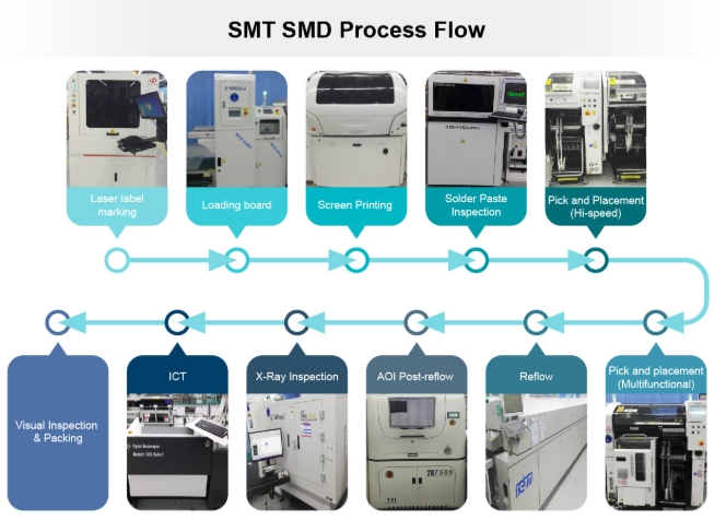
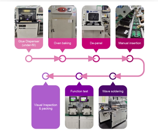
SMT Process Flow Diagrams
- SMT Surface Mount Device (SMD) Process Flow
- SMT Through-Hole Device (DIP) Process Flow
Key Inspection Technologies in SMT PCB Assembly
AOI (Automatic Optical Inspection)
AOI automates PCB visual inspection by comparing images of tested boards to reference images to identify defects. AOI offers greater accuracy than manual inspection and is widely used before and after reflow soldering.
Advantages:
- Replaces manual visual inspection
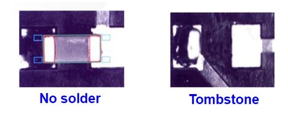
- Detects defects such as missing components, skew, tombstoning, wrong parts, polarity reversal, lifted leads, solder bridges, insufficient solder, and cold solder joints
Limitations:
- May cause false rejects due to shadows or subtle grayscale variations
- Cannot inspect hidden solder joints beneath components or shields (requires AXI)
To explore AOI and related inspection systems, visit BUYSMT AOI Equipment.
ICT (In-Circuit Test)
ICT tests the electrical properties of assembled PCBs without removing components, using needle probes contacting predefined test points.
Advantages:
- Fast and accurate electrical testing of components and nets
- Reduces false and missed defects
- Minimizes manual operations and costs
- Helps rapidly locate faulty components for repair
Limitations:
- High fixture and equipment costs, suitable for large volume production
- Requires test point design on PCB
- Probe maintenance is critical for reliable testing
ICT complements AOI by detecting electrical defects that AOI cannot see.
Common SMT Defects Detectable by AOI and ICT
- Missing components
- Component skew or offset
- Tombstoning (standing components)
- Wrong or reversed polarity parts
- Lifted or bent leads
- Solder bridges
- Insufficient solder
- Cold or false solder joints
For a full range of SMT production line equipment and professional support, visit BUYSMT SMT Solutions.